Find the right thermal pad →
Your devices run hot.
Let's fix that.
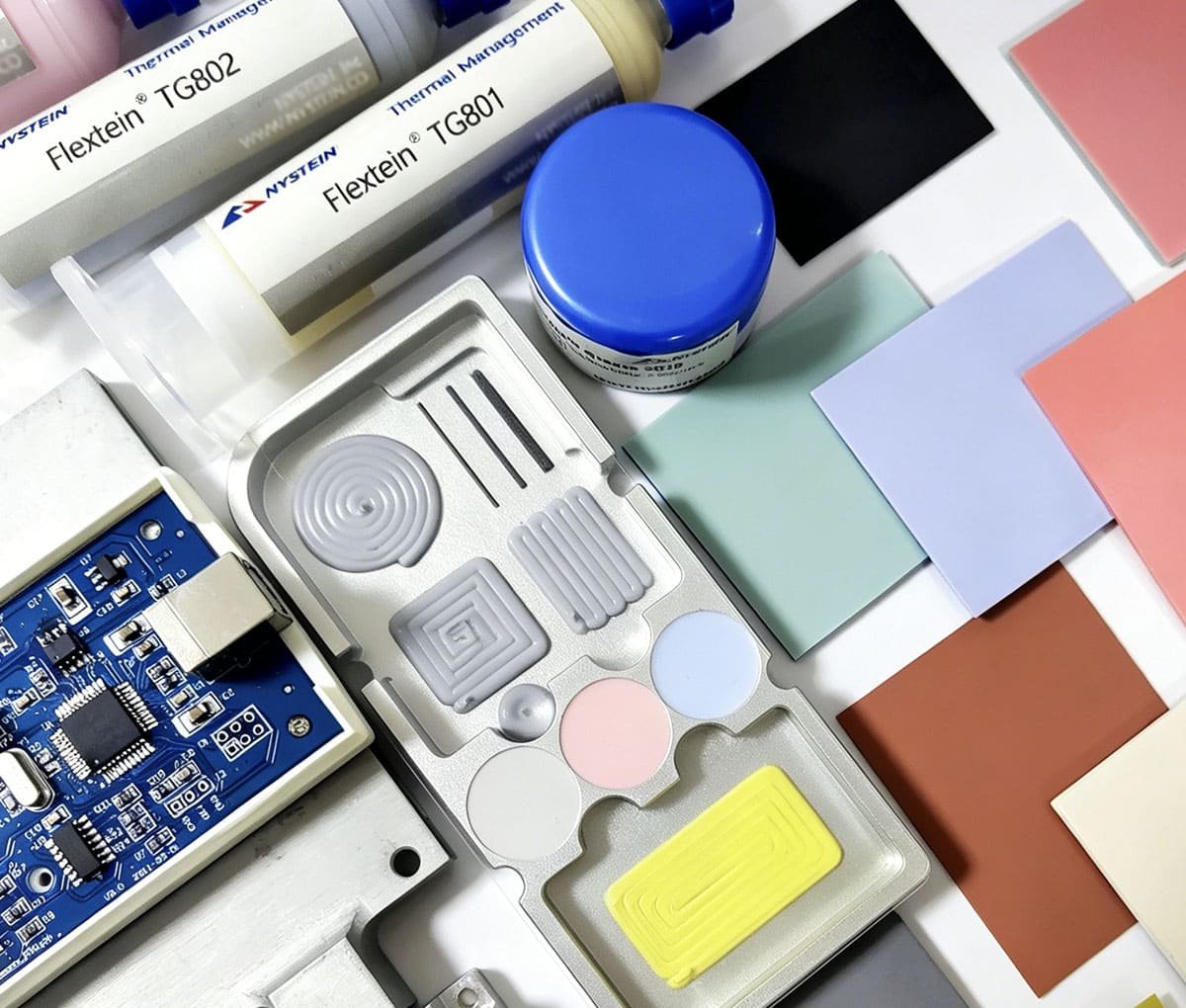
Kleber's Flextein gap pad series covers 1.5-15 W/m·K, from consumer electronics to AI data centers and embodied AI robots. One trusted supplier, full thermal chain.
Up to 15 W/m·K
IATF 16949 · ISO 9001
15 W/m·K
Max thermal conductivity
20+ SKUs
Flextein series
−40 ~ 150 °C
Operating range
0.3 - 10 mm
Custom thickness
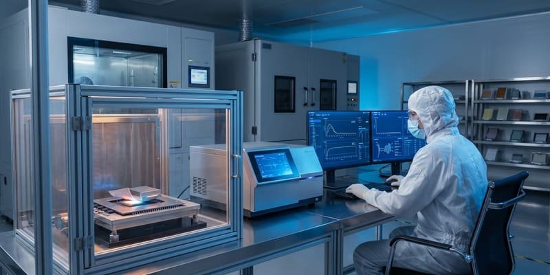
We go deep into your application.
Kleber's AE team works from your product structure level -- not a generic solution off the shelf.
Device throttling due to overheating
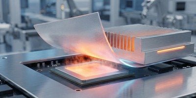
Insufficient conductivity traps heat between chip and heatsink.
Flextein spans 1.5-15 W/m·K to match every power density precisely.

Too many suppliers, high procurement cost
Pads, gels, phase-change materials from different vendors -- complex reconciliation.
Kleber supplies the full thermal chain -- your entire BOM from one source.

Strict EU/US certifications, hard to prepare
RoHS / REACH / UL94 all required -- long cycle, high rejection risk.
Full series RoHS & REACH compliant; CNAS lab issues third-party reports on demand.
Silicone oil migration contaminates precision contacts
Thermal cycling causes silicone bleed-out, fouling optical modules and sensors.
S8000 silicone-free series -- zero contamination for optical, aerospace, telecom, and robotics.
Standard products don't fit special applications
Medical, UAV, OPC, and robotics joints need unique low-stress, low-volatility formulas.
Kleber AE team reverse-engineers custom formulations from your scenario.

Supplier data unverifiable, switching risk is high
No independent test basis for design decisions.
CNAS-certified lab runs 24/7; competitive benchmark reports available on request.

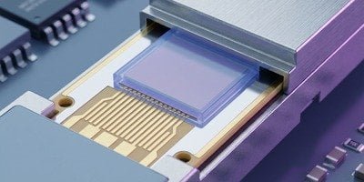
AI Data Center — Dedicated Thermal Solution
As AI GPU power exceeds 700W, Kleber offers full-chain thermal coverage from chip to rack level.

Embodied AI robots — the next thermal frontier
Ultra-thin, low-stress, silicone-free materials engineered for robotic bodies where data-center heat density meets centimeter-scale space constraints.
Full coverage, from chip to cabinet
Six product categories — one supplier. Select by material type.
Flextein S20
2.0 W/m·K
Cost-efficient soft gap pad with double-sided natural tack. Go-to entry choice for consumer electronics, LED lighting, and general-purpose power modules.
Flextein S80H
8.0 W/m·K
Ultra-soft (Shore OO 45) and ultra-high conductivity. Fills micro-surface gaps under minimal compression. D3–D20 = 0 ppm. Primary choice for AI servers, EV battery modules, and robotic joint drives.
Flextein S150
15.0 W/m·K
Highest conductivity in the Flextein pad lineup. For the most power-dense chips — high-end GPUs, AI accelerators, and on-board inference modules.
Flextein S60T
6.0 W/m·K
Ultra-thin pad with PI or glass-fiber substrate. At 0.15 mm delivers ≥ 5 kV breakdown — thermal conduction and electrical isolation in one component.
Flextein S8000
8.0 W/m·K
Zero silicone — no D3–D20 contamination, no oil migration. Built for optical transceivers, telecom, aerospace, and embodied AI sensor systems.
TG880 & KB-PCM850
8.0 – 8.5 W/m·K
Two flowable formats for variable-gap assemblies. TG880 is a dispensable cross-linked gel. KB-PCM850 melts at 50°C achieving 0.007 mm bond line.
Thermal conductivity range (W/m·K)
ISO 22007-2 · ASTM D5470ISO 22007-2 or ASTM D5470
Not sure which conductivity fits your design?
AE team recommends within 24h — free of chargeFlextein S15SS
1.5 W/m·K
Ultra-soft Shore OO 7. Low density, low oil permeability. Ideal for battery cooling where conformability at low pressure matters.
Flextein S20
2.0 W/m·K
Cost-efficient silicone-based pad with double-sided tack. Standard 470×470 mm. High reliability, re-workable.
Flextein S30FP
3.0 W/m·K
Low-stress, low-volatile. D3–D20 ≤ 50 ppm. Shore OO 25. Medical and UAV applications.
Flextein S80H
8.0 W/m·K
Ultra-soft Shore OO 45. D3–D20 = 0 ppm. Excellent compressibility under low force.
Flextein S100
10.0 W/m·K
Ultra-high conductivity gap pad. Good compressibility. Oil seepage <1% at 125°C/48h.
Flextein S150
15.0 W/m·K
Highest conductivity in the lineup. Oil seepage <1% at 125°C/48h. Natural tack both sides.
Flextein S180
18.0 W/m·K
The absolute highest conductivity — 18 W/m·K. For extreme power-density applications.
Flextein S60T
6.0 W/m·K
Ultra-thin pad with PI or glass-fiber substrate. At 0.15 mm delivers ≥ 5 kV (PI) or ≥ 3 kV (glass fiber) breakdown. Thermal and electrical isolation in one component.
Flextein S2000
2.0 W/m·K
Entry-level silicone-free pad. Pink color, natural tack both sides. Low modulus, no oil penetration.
Flextein S4000
4.0 W/m·K
Blue-purple silicone-free pad for telecom and aerospace. Low volatiles, excellent dielectric.
Flextein S8000
8.0 W/m·K
Highest-conductivity silicone-free pad. Zero D3–D20, zero oil migration. TML ≤ 1.0%. Benchmark for optical, aerospace, and embodied AI.
Flextein TG802
2.0 W/m·K
Entry-level cross-linked gel. No pump-out, no settling. Re-workable.
Flextein TG880
8.0 W/m·K
High-conductivity cross-linked gel. No cure, no pump-out. Superior long-term stability.
Flextein TG892
12.0 W/m·K
Ultra-high 12 W/m·K gel. Non-settling, non-flowing. D3–D20 < 50 ppm.
KB-PCM850
8.5 W/m·K
Melts at 50°C. Bond line 0.007 mm. Lowest thermal resistance in the Kleber lineup: 0.03 °C·cm²/W.
Not sure which pad fits your design?
Our engineers reply within 24 hours.
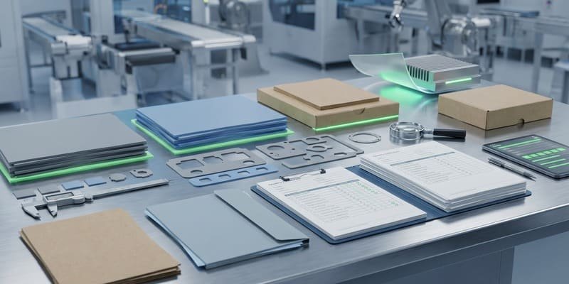
Built for engineers, certified for buyers
Every Kleber product ships with full technical documentation and independent lab-verified data.
CNAS-certified lab
24/7 in-house lab. Third-party competitive benchmark reports on request.
RoHS & REACH compliant
EU environmental requirements met across full range. Recyclable packaging standard.

UL 94 V-0 flame rated
Full Flextein series passes V-0. Safe for automotive, medical, industrial, and robotics.
Re-workable assembly
Double-sided natural tack. Peel and reposition without residue.
Custom thickness & die-cut
0.3–10 mm. Sheets or die-cut parts. Flexible MOQ for qualification.
One-stop thermal supply
Pad, gel, phase change, graphite — full thermal BOM from Kleber alone.
Ready to test Kleber materials in your application?
Free samples · Full TDS · AE support includedNot a trading company. A manufacturer with labs, lines, and engineers.
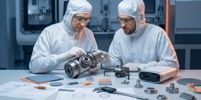
Every Kleber product is developed, tested, and manufactured in-house.

In-house R&D team
Custom formulations from your actual product structure. Validated in our own lab before shipment.
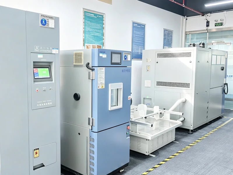
Reliability lab
Thermal shock, humidity aging, flame testing — all in-house. CNAS L23188 accredited. Reports on demand.
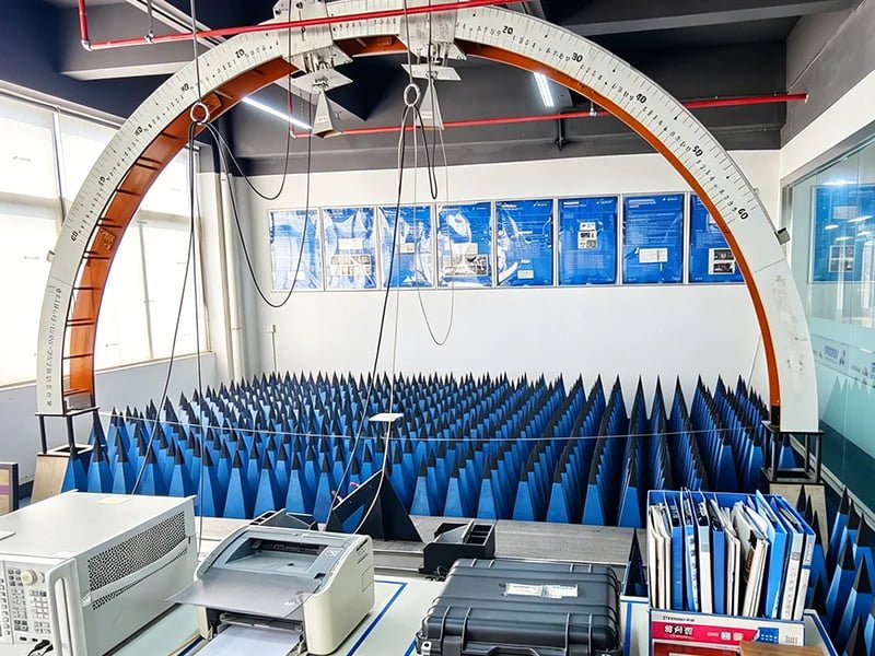
EMI test chamber
In-house anechoic chamber, 300 MHz to 40 GHz. Same lab that validates materials for Nokia and Ericsson.
Manufacturing infrastructure
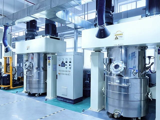
Large-scale mixing and compounding equipment.
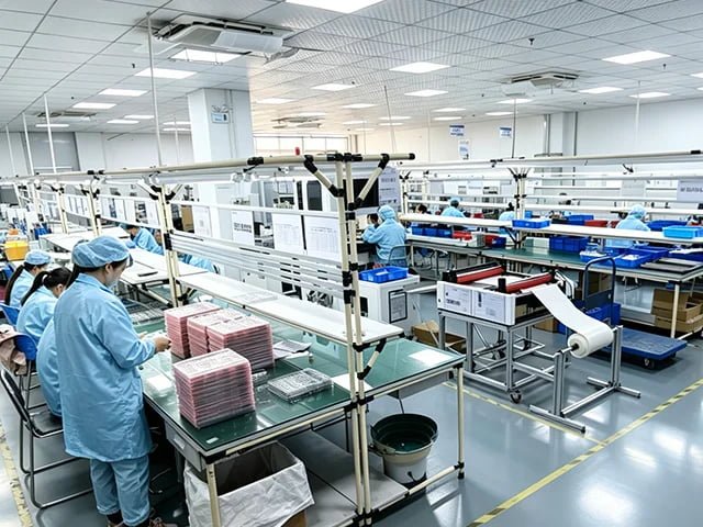
EMI shielding and precision die-cut materials.
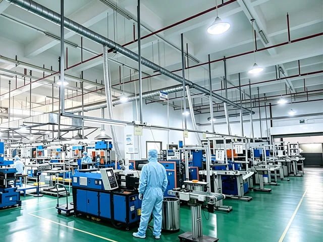
Dedicated high-volume line. Standard and custom.

Every batch checked under cleanroom conditions.
CNAS L23188
Accredited lab
24/7
Lab hours
300 MHz–40 GHz
EMI range
3
Production bases

Our AE team works on your problem, not on a product sheet.
When a customer in the optical module space came to us with a silicone contamination issue after 2,000 thermal cycles, our AE team rebuilt the formulation from the interface geometry up. That's what the S8000 series came from.
Talk to an engineerTrusted across industries
Kleber thermal materials tested and validated in the most demanding environments worldwide.
Not sure which product fits?
Tell us your requirements. Our engineers respond within 24 hours.
Send us your requirements
We'll match you with the right thermal solution within 24 hours.